Electronic Device And Electronic Circuit

Data of electronic device , PCB Design and electronic circuit

Google
 
Web basicelectronic.blogspot.com

Tuesday, March 31, 2009

Switch Protection Design - Fast-Recovery Diodes


Abstract
The number of fast recovery applications in high power systems
continues to grow leading to various dynamic constraints and
hence different diode designs and behaviours. Along with
conventional RC (“SCR-type”) and C (“GTO-type”) snubber
conditions, snubberless conditions in both IGBT and IGCT
applications are gaining ground at ever higher currents and
voltages (presently 6 kV). Within these two groups, the further
distinctions of “inductive” and “resistive” commutation di/dt must
be made for an optimal diode design. Diodes capable of high
reverse di/dt and dv/dt can today be realised thanks to controlled
life-time profiling which will be described here with both measured
and simulated results. As will also be explained, such “robust”
designs, though essential for snubberless operation, may be “less
robust” under snubbered conditions so that a clear understanding
of the application (Snubber, Free-Wheel, Clamp, Resistive or
Inductive di/dt) is required for the correct choice or design of a fast
recovery diode. The different diode commutation conditions will
be described and categorised and the optimal diode design
identified with supporting measurements and simulations.


Fig 2 “Inductive” commutation circuit fitted
with snubber and clamp

Traditionally the diode under consideration (in this case a
Free-Wheel Diode (FWD)) is fitted with a snubber and may also
be fitted with a clamp as shown in Fig. 2. Thus for the inductive
commutation circuit, we can define the additional sub-conditions
consisting of permutations of the snubbered/unsnubbered &
clamped/unclamped conditions whereby the snubber controls
the Duet’s dv/dt whereas the clamp controls its peak voltage.

More pdf

Labels: ,

Sunday, March 29, 2009

Mosfet Snubber Circuit in Flyback Converter Circuit

Mosfet Protection in flyback Circuit


PKC-136

PEAK CLAMP

CHARACTERISTICS
VBR 160Vdc
VDRM 700Vdc
P 1.5W

Feature
- Protection of the Mosfet in flyback power supply
- TRANSIL™ and blocking diode in a single
package

BENEFITS

- Accurate voltage clamping regardless load
- Reduced current loop
- Reduced EMI emission
- High integration
- Fast assembly
- Reduced losses in stand by mode

PKC-136 datasheet pdf


Mosfet Snubber Circuit in Flyback Converter


Fig. 1 Typical flyback convertor with drain clamping circuits

ZenBlock
Zener with integrated blocking diode
Philips Semiconductors' new ZenBlockTM replaces
double-diode-, RCD- or RC-snubbers in flyback convertors.
The new components offer circuit designers the important
benefits of lower component count and board usage, reduced
EMI, optimal clamping at all loads and higher efficiency.

Introducing

The new ZenBlock combines the double diode snubber in one
package. This leads to the following advantages:
-Fewer components.
-Reduced circuit board space
-Lower EMI by reducing the drain clamp circuit length and
area.
-Optimal clamp performance at all loads (compared with RCD
and RC snubber)
-Higher efficiency at low loads (compared with RCD and RC
snubber)

ZenBlock datasheet pdf

Labels: ,

Friday, March 27, 2009

Push-Pull Snubber Circuit

Abstract
The DS3984, DS3988, DS3881, DS3882, DS3992, and DS3994
are cold-cathode fluorescent lamp (CCFL) controllers that use a
push-pull architecture to create the high-voltage AC waveforms
needed to drive the lamps. In a push-pull drive scheme, the
parasitic inductance of the step-up transformer, together with the
parasitic capacitance of the output of the n-channel power
MOSFETs, form a resonant circuit that can create unwanted
voltage spikes. High-voltage spikes can increase the stress on
the power MOSFETs and can also increase the electromagnetic
interference (EMI) created by the system. This application note
describes how to suppress the voltage spikes with a simple
resistor-capacitor (RC) network.

Push-pull drain snubber circuit.


Labels: ,

Wednesday, March 25, 2009

Design the MOSFET RCD Snubber Circuit

When the power MOSFET is turned off, there is a high
voltage spike on the drain due to the transformer leakage
inductance. This excessive voltage on the MOSFET may
lead to an avalanche breakdown and eventually failure of the
FPS. Therefore, it is necessary to use an additional network
to clamp the voltage.

The RCD snubber circuit and MOSFET drain voltage
waveform are shown in Figure 10 and 11, respectively. The
RCD snubber network absorbs the current in the leakage
inductance by turning on the snubber diode (Dsn) once the
MOSFET drain voltage exceeds the voltage of node X as
depicted in Figure 10. In the analysis of snubber network, it
is assumed that the snubber capacitor is large enough that its
voltage does not change significantly during one switching
cycle. The snubber capacitor used should be ceramic or a
material that offers low ESR. Electrolytic or tantalum
capacitors are unacceptable due to these reason

Circuit diagram of the snubber network

The first step in designing the snubber circuit is to determine
the snubber capacitor voltage at the minimum input voltage
and full load condition (Vsn). Once Vsn is determined, the
power dissipated in the snubber network at the minimum
input voltage and full load condition is obtained as


where Ids-peak is specified in equation (8), fs is the FPS
switching frequency, Llk is the leakage inductance, Vsn is the
snubber capacitor voltage at the minimum input voltage and
full load condition, VRO is the reflected output voltage and
Rsn is the snubber resistor. Vsn should be larger than VRO
and it is typical to set Vsn to be 2~2.5 times VRO. Too small a
Vsn results in a severe loss in the snubber network as shown
in equation (23). The leakage inductance is measured at the
switching frequency on the primary winding with all other
windings shorted.
Then, the snubber resistor with proper rated wattage should
be chosen based on the power loss. The maximum ripple of
the snubber capacitor voltage is obtained as


where fs is the FPS switching frequency. In general, 5~10%
ripple of the selected capacitor voltage is reasonable.
The snubber capacitor voltage (Vsn) of equation (26) is for
the minimum input voltage and full load condition. When
the converter is designed to operate in CCM under this
condition, the peak drain current together with the snubber
capacitor voltage decrease as the input voltage increases as
shown in Figure 11. The peak drain current at the maximum
input voltage and full load condition (Ids2 peak) is obtained as

where Pin, and Lm are specified in equations (1) and (6),
respectively and fs is the FPS switching frequency.
The snubber capacitor voltage under maximum input voltage
and full load condition is obtained as


where fs is the FPS switching frequency, Llk is the primary
side leakage inductance, VRO is the reflected output voltage
and Rsn is the snubber resistor.

Figure 11. MOSFET drain voltage and snubber
capacitor voltage

From equation (26), the maximum voltage stress on the
internal MOSFET is given by


where VDC max is specified in equation (3). Check if Vds
max is below 85% of the rated voltage of the
MOSFET (BVdss) as shown in Figure 12. The voltage rating
of the snubber diode should be higher than BVdss. Usually,
an ultra fast diode with 1A current rating is used for the
snubber network.

In the snubber design in this section, neither the lossy
discharge of the inductor nor stray capacitance is considered.
In the actual converter, the loss in the snubber network is

Less than the designed value due to this effects


Source
Design Considerations for Battery Charger Using
Green Mode Fairchild Power Switch (FPSTM)

http://www.fairchildsemi.com/an/AN/AN-4138.pdf

Labels:

Monday, March 09, 2009

Mosfet RCD Snubber Circuit Design

Design Guidelines for RCD Snubber of Flyback Converters
Application Note AN-4147
Fairchild Semiconductor
Snubber design
The excessive voltage due to resonance between Llk1 and
COSS should be suppressed to an acceptable level by
an additional circuit to protect the main switch.


The RCD snubber
circuit and key waveforms are shown in Figures 2 and 3.
The RCD snubber circuit absorbs the current in the leakage
inductor by turning on the snubber diode (Dsn) when Vds
exceeds Vin+nVo. It is assumed that the snubber capacitance
is large enough that its voltage does not change during one
switching period.


When the MOSFET turns off and Vds is charged to Vin+nVo,
the primary current flows to Csn through the snubber diode
(Dsn). The secondary diode turns on at the same time.
Therefore, the voltage across Llk1 is Vsn-nVo. The slope of
isn is as follows:

more(pdf)

Snubber Circuits Suppress Voltage Transient Spikes in
Multiple Output DC-DC Flyback Converter Power Supplies
RCD Voltage Snubber
This snubber is applicable to rate-of-rise voltage control
and/or clamping. The presence of the diode in the
configuration makes this a polarized snubber. The two
possible configurations for this resistor-capacitor-diode
(RCD) snubber are shown in Figure 2. The configuration
shown in Figure 2A can only act as a voltage clamp.
The variation shown in Figure 2B is applicable to either
rate-of-rise control or clamping of the drain voltage of
the switch.

RCD Clamp
In the clamp mode the purpose of the snubber is to
clamp the voltage during turn-off at the drain of the
MOSFET. The parallel RC circuit may be returned to
ground or to a voltage other than ground (i.e., input voltage
if the drain can go above input voltage) since this will
reduce the power dissipation in the resistor. The MOSFET
switch itself will have to sustain the peak power dissipation
during turn-off. The value of the capacitor, CCLAMP,
and resistor, RCLAMP, is based on the energy stored in
the parasitic inductance, as this energy must be
discharged into the RC network during each cycle.
The voltage across the capacitor and resistor sets the
Clamp voltage, VCLAMP.


Rate-of-Rise Control RCD Snubber
When the RCD snubber is used to control the rate of
voltage rise at the MOSFET drain, the capacitor must be
completely charged and discharged during each cycle to
be able to control the rate-of-rise of the drain voltage.
The RC time constant of the snubber should, therefore,
be much smaller than the switching period (consider the
effect of duty cycle on pulse width). Typically, the time
constant should be about 1/10th the switching period.
When the switch turns off, the inductor current is diverted
through the snubber diode to charge the capacitor to
the rail. At that time, it is expected that the output rectifier
will turn on.


more(pdf)

MAGNETIC SNUBBER FOR 200W PFC
WITH UNIVERSAL MAINS
In high voltage continuous mode boost converters,
a significant part of the power mosfet switching
losses is related to the turn-on edge.
In fact, at turn on, the power mosfet has to sustain
both the boost diode reverse recovery and
the stray capacitances associated energies.
Moreover, the additional peak current due to the
recovery of the diode can be significantly high, in
particular at high temperature, thus increasing the
high frequency noise, the E.M.I. filter requirements
and reducing efficiency.
The turn on peak current, generating all the
above mentioned problems, has been dramatically
reduced by using the magnetic snubber we
propose at Fig. 1b.
The concept of this snubber is to reduce (and
control) the turn-on di/dt of the mosfet to the most
convenient value, considering the voltages and
switching frequency applied to the system.

Voltage Snubber

Labels: , ,

Thursday, March 05, 2009

Inductor Design


Filter inductor design constraints
Objective:
Design inductor having a given inductance L,
which carries worst-case current Imax without saturating,
and which has a given winding resistance R, or,
equivalently


Index
- Assumed filter inductor geometry
- Constraint: maximum flux density
- Constraint: Inductance
- Constraint: Winding area
- The window utilization factor Ku
- also called the “fill factor”
- Winding resistance
- The core geometrical constant Kg
- Core geometrical constant Kg
- A step-by-step procedure
more (pdf)


INDUCTOR DESIGN in SWITCHING REGULATORS
Technical Bulletin
Better efficiency, reduced size, and lower costs have combined to
make the switching regulator a viable method for converting unfiltered
DC input voltages into regulated DC outputs. This brochure describes
the switching regulator and presents design information. In particular,
MAGNETICS® Ferrite and Molypermalloy Powder cores used for
the power inductor are highlighted.

DESCRIPTION


A typical circuit consists of three parts: transistor switch, diode
clamp, and an LC filter. An unregulated DC voltage is applied to
the transistor switch which usually operates at a frequency of 1 to 50
kilohertz. When the switch is ON, the input voltage, Ein, is applied to
the LC filter, thus causing current through the inductor to increase;
excess energy is stored in the inductor and capacitor to maintain
output power during the OFF time of the switch. Regulation is
obtained by adjusting the ON time, ton, of the transistor switch, using
a feedback system from the output. The result is a regulated DC
output,

index
- COMPONENT SELECTION
- INDUCTOR DESIGN
- CORE SELECTION PROCEDURE
- DESIGN EXAMPLE
Switching Regulator Inductor Design
COILTRONICS Application Notes Magnetics
In switching regulator applications the inductor is used as
an energy storage device, when the semiconductor
switch is on the current in the inductor ramps up and
energy is stored. When the switch turns off this energy is
released into the load, the amount of energy stored is
given by;
Energy = 1/2L.I2 (Joules) (1)
Where L is the inductance in Henrys and I is the peak
value of inductor current.
The amount by which the current changes during a
switching cycle is known as the ripple current and is
defined by the equation;
V1 = L.di/dt (2)
Where V1 is the voltage across the inductor, di is the
ripple current and dt is the duration for which the voltage
is applied. From this we can see that the value of ripple
current is dependent upon the value of inductance.
Choosing the correct value of inductance is important in
order to obtain acceptable inductor and output capacitor
sizes and sufficiently low output voltage ripple.


Index
- Inductor Selection for Buck Converters
- Inductor Selection for Boost Converters
- Inductor Selection for Buck-Boost Converters

Labels: , ,

Monday, March 02, 2009

Gate Drive for step-down switching regulator

CDV/DT INDUCED TURN-ON IN SYNCHRONOUS BUCK
REGULATORS
Abstract
Cdv/dt induced turn-on of the synchronous MOSFET deteriorates
performance in synchronous buck regulators. We will discuss this
problem and provide several solutions that can reduce the effects.
BIPOLAR OR CMOS GATE DRIVER?
An in-circuit waveform showing the Cdv/dt induced
turn-on effect at Q2 gate is demonstrated in Figure 7. The
gate drive circuit might further deteriorate this Cdv/dt
induced turn-on problem. It is clear in Figure 7 that the
gate driver can only pull the gate voltage of Q2 down to
0.7V, instead of zero, when Q2 is turned off. However, the
Cdv/dt induced voltage is sitting on top of this turn-off
gate voltage and makes Q2 more vulnerable to the Cdv/dt
induced turn-on problem. The gate driver used in Figure 7
is created by a bipolar process.


http://www.irf.com/technical-info/whitepaper/syncbuckturnon.pdf

“Shoot-through” in Synchronous Buck Converters
Abstract

The synchronous buck circuit is in widespread use to
provide “point of use” high current, low voltage
power for CPU’s, chipsets, peripherals etc. In the
synchronous buck converter, the power stage has a
“high-side” (Q1 below) MOSFET to charge the
inductor, and a “Low-side” MOSFET which replaces
a conventional buck regulator’s “catch diode” to
provide a low-loss recirculation path for the inductor
current.


Shoot-through is defined as the condition when both
MOSFETs are either fully or partially turned on,
providing a path for current to “shoot through” from
VIN to GND. To minimize shoot-through,
synchronous buck regulator IC’s employ one of two
techniques to ensure “break before make” operation
of Q1 and Q2 to minimize shoot-through:

1. Fixed “dead-time”: A MOSFET is turned off,
then a fixed delay is provided before the lowside
is turned on. This circuit is simple and
usually effective, but suffers from its lack of
flexibility if a wide range of MOSFET gate
capacitances are to be used with a given
controller. Too long a dead-time means high
conduction losses. Too short a dead time can
cause shoot-through. A fixed dead-time
typically must err on the “too long” side to allow
high CGS MOSFETs to fully discharge before
turning on the complementary MOSFET.

2. Adaptive gate drive: This circuit looks at the
VGS of the MOSFET that’s being driven off to
determine when to turn on the complementary
MOSFET. Theoretically, adaptive gate drives
produce the shortest possible dead-time for a
given MOSFET without producing shootthrough.
In practice, a combination of adaptive and fixed
produces the best results, and is typically what is in
today’s PWM controllers and gate drivers as shown
in Figure 2


http://www.fairchildsemi.com/an/AN/AN-6003.pdf

A New Hybrid Gate Drive Scheme for High
Frequency Buck Voltage Regulators

Abstract
This paper presents a new hybrid drive scheme
for a synchronous buck voltage regulator (VR). The
proposed current-source driver is used to drive the control
MOSFET to achieve fast switching speed and reduce the
switching loss significantly due to the parasitic inductance in
addition to gate energy recovery. Conventional voltage
driver is used for synchronous rectifier (SR) MOSFET for
its simplicity and good immunity and alleviation of dv/dt
effect. The experimental results prove the advantages of the
new drive scheme and a significant efficiency improvement
has been achieved. At 1.3 V output, the new driver improves
the efficiency from 82.8% using a conventional driver to
85.6% (an improvement of 2.8%) at 20 A, and at 25 A, from
80.5% to 83.0% (an improvement of 2.5%). The new drive
can also be integrated into a standard drive integrated
circuit (IC) and replace the conventional voltage drive IC
directly. Overall, the new driver scheme is very promising
from the standpoints of both performance and costeffectiveness.

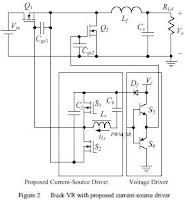
Figure 2 shows the buck converter with the proposed
hybrid drive circuit. The key waveforms are shown in
Figure 3. Essentially, the new high-side current-source
driver is used for the control MOSFET to achieve fast
switching transition. It consists of two driver MOSFETs
S1 and S2, a bipolar transistor pair S3 and S4, the resonant
inductor Lr, the bootstrap capacitor Cf , diode Df and the
blocking capacitor Cb. Vc are the drive voltages. Cgs1 and
Cgs2 are the input gate capacitors of MOSFETs Q1 and Q2
respectively. S1 and S2 are switched out of phase with
complimentary control respectively.


Labels: , ,