Electronic Device And Electronic Circuit

Data of electronic device , PCB Design and electronic circuit

Google
 
Web basicelectronic.blogspot.com

Monday, December 05, 2011

Home made UV PCB exposure box

Examples and guidelines on how to do UV PCB exposure box by your self

UV LED PCB Exposure System


Home made UV LED PCB exposure box PCB exposure box made with large array of UV LEDs This project shows the creation of a large array of UV LEDs. They are used to expose a presensititised blank circuit board. Another common method is to use UV tubes. Alfredo has translated it to English as well as he could
more

Ultraviolet light source UV-80 for PCB exposure
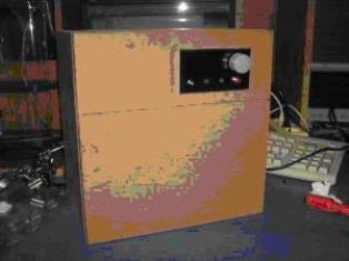
Home made UV light PCB exposure box PCB exposure box made with Ultraviolet light for Double side PCB exposure


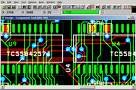
One of more advanced PCB manufacturing methods is exposing laminate copper boards covered by photo resistive layer through mask. Using UV light in manufacturing PCB has many benefits according to other methods: you can get thin tracks like 0.2mm. You could do this by using other home techniques like laser printers or hand artwork
more

Single LED UV PCB exposure box 
Home made UV LED PCB exposure box PCB exposure box made with Single LED UV LZ1-10UA05


Having seen several attempts to make a PCB exposure box with LEDs instead of tubes, i decided to make my own. I wanted a smal one because i make prototypes one of a kind pcbs, and they are always small. Other projects i saw are using a large number of low power uv leds wich are in the miliwatt range. 80 Leds seems to be the minimum number to achieve 1W of UV radiated power, wich is what is needed to expose the PCB in a decent time.
more

Building a UV exposure box
Home made UV LED PCB exposure box PCB exposure box made with array of UV LEDs for Double side PCB exposure


There are two methods of using etchant resist when making circuit boards. We use the toner transfer method that requires ironing on laser toner to the copper, but you can also use chemical resist that reacts to ultraviolet light. [Bogdan] decided to start doing more of the latter so he built a UV exposure box to make the process easier.
more

PCB Photographic Artwork Transfer UV Cabinet 


Until now, to transfer the artwork to a photosensitive board, i used a pair of UV lamps. Although they worked pretty well, i thought of upgrading my lab. Thus, i designed and made a prototype photographic artwork transfer box using UV LEDs:
more

LED and Black light UV Light

Labels: ,

Wednesday, June 15, 2011

Solar Power Center and Solar Charger Circuit

Solar Power Center and Solar Charger Circuit

TLC2272 - 10 Amp out Solar Power Center
The SPC3 is a solar power center, it can handle all of the power functions for a solar charged 12 Volt DC system. The SPC3 contains a 9 amp photovoltaic charge controller, a 10 amp low voltage load disconnect circuit and a built-in white LED array for area illumination. The low voltage disconnect circuit has a load on-off switch, and a battery low voltage indicator. By using the SPC3 as the center of a solar powered device, long battery life is assured. The SPC3 can be used as a self-contained solar lighting system, it is also useful for making solar powered audio and radio devices and much more.
Specifications
Charge Controller Theory
Low Voltage Disconnect Theory
Charge Controller Alignment
Low Voltage Disconnect Alignment
SPC3 Circuit Extensions
more


AA Battery Solar Charger

Each of the solar cells develops about 0.5 volts across itself when in full sunlight. The string of 8 solar cells puts out around 4V with no load. When the solar cells are connected to a battery, a current will flow and the battery will charge.
Two versions of the circuit are shown in the schematic, the 8 solar cell panel with a diode is the recommended circuit. The diode prevents the battery from discharging through the cells at night and the 8th cell boosts the voltage up enough to compensate for the voltage drop across the diode. For an 8 solar cell panel, connect jumper J2 and disconnect J1. For a 7 solar cell panel, connect jumper J1 and eliminate SC8 and D1. Typically, the jumpers are not necessary, they are shown in the schematic to illustrate two ways to to build the circuit.
For operation in cloudy weather, it may be useful to add one or two additional solar cells. It is a good idea to temporarily insert an amp (microamp) meter in series with the battery to measure the charging current in various light conditions.
Since solar cells are current-limited devices, it is possible to use the circuit as-is to charge a single battery cell. If one cell is all you ever need to charge, five solar cells and a series diode will be sufficient for the task.
more


Solar charger for lead-acid batteries.

This circuit is intended for charging sealed lead-acid batteries with a solar panel in small and portable applications. The customary diode that prevents the battery from discharging through the solar panel has been replaced by a FET-comparator combination. The charger will stop charging once a pre-set voltage (temperature compensated) has been reached, and recommence charging when the voltage has dropped off sufficiently. The load is disconnected when the battery voltage drops below 11V and reconnected when it gets back to 12.5V.
more


SOLAR CHARGER
he circuit is a single transistor oscillator called a feedback oscillator, or more accurately a BLOCKING OSCILLATOR. It has 45 turns on the primary and 15 turns on the feedback winding. There is no secondary as the primary produces a high voltage during part of the cycle and this voltage is delivered to the output via a high-speed diode to produce the output. The output voltage consists of high voltage spikes and should not be measured without a load connected to the output. In our case, the load is the battery being charged. The spikes feed into the battery and our prototype delivered 30mA as a starting current and as the battery voltage increased, the charging current dropped to 22mA.
more

Labels: ,

Thursday, February 04, 2010

Basic Levitation and Magnetic Levitation Circuit Project

Understanding Basic Levitation
In basic levitation (Fig 1) an object appears to float due to the invisible forces of magnets. A magnet creates a field that forms two opposing poles: North and South (Fig 2). Opposite poles attract each other while similar poles repel. For magnetic levitation, there is a fixed magnet and a smaller free moving permanent magnet, which is the object that will levitate. This object has two forces exerted on it: downward force from gravity and upward force from the fixed magnet.
http://icb.olin.edu/spring_04/ttgb/student/Ukiyo/understanding.htm


Magnetic Levitation Schematic Circuit


more


Levitation Photodetector Circuit
This optodetector measures the position of the ball by the amount of light transmitted by the infrared LED. This is a linear signal across the small area of the detector -- it is not just "on" and "off".


Levitation Difference Amplifier Circuit
This circuit creates a control signal from the two optodetectors. It finds the difference between the two input voltages and amplifies it to get the ball's position. This stage is often called a comparator.


Levitation Output Amplifier Circuit
This circuit amplifies the control signal in preparation for the power output transistor. Why do we need this stage at all? Because we reduced the whole signal by one-ninth in the speed-plus-position circuit.

more


Perpetual top Levitation Toy
The point of the perpetual top levitation toy is simply that it continues spinning forever, and the challenge is to understand the driving mechanism. The top is made of plastic, and contains embedded in it a small permanent magnet, oriented perpendicular to the spin axis of the top. The base contains a transistor and a coil with two windings, the assembly being driven by a 9-volt power supply. A schematic of the electrical circuit is shown in the figure.
As one pole of the magnet (say the south pole) approaches the coil, a current in induced in winding A, in such a direction as to make the base of the transistor (an NPN) go positive. That makes the emitter-collector current flow through winding B, in the opposite direction to A. The current through B is larger than that of A (due to the amplification of the transistor), so by Lenz's law the magnet pole will be attracted to the coil.


more


Magnetic Levitation Circuit
This is a simple magnetic levitator circuit which suspends objects a set distance below an electromagnet. The physics behind it is to simply provide a magnetic force which equal and opposite to the gravitational force on the object. The two forces cancel and the object remains suspended. Practically this is done by a circuit which reduces electromagnet force when an object gets to close, and increases it when the object is out of range.


more


MAGNETIC LEVITATION Project & CRITICAL TEMPERATURE KIT
ELECTRONICS CIRCUIT SCHEMATIC DIAGRAMS
The following figure is a schematic diagram for the Electronics Board.


Operation of the Electronics Board circuitry may be of interest to some students who use the Levitation/Critical Temperature kit. Individual circuit functions may be understood and analyzed from the following explanations. Operational amplifiers (op amps) are characterized by two nearly ideal properties, which lead to a wide variety of applications. These properties are 1) high impedance between the non-inverting and inverting inputs and 2) high open loop gain. Usually, both of these may be assumed to be infinite. Infinite impedance means no current flows between inputs, and infinite gain means that negative feedback will drive input voltage difference to zero. A variety of circuits can be analyzed using these two properties and Ohm's law.
more

Labels: ,

Wednesday, December 30, 2009

Wireless Dimmer Circuit Project


AVR wireless dimmer Project
At first we have to modify the layout of the old Avr dimmer. I don't think the RS232 interface will be used much when we have the wireless option available, so all the parts for the RS232 will have to go, the other thing that we don't really need anymore is the crystal with the 2 capacitors, because the ATtiny2313 has a build in RC clock of 4 and 8 Mhz which is more than sufficient. One more thing that could go is the infrared receiver, but this doesn't take much room on the circuit board so I will leave it on for the moment. The last thing we need to change is the power supply. The iDwaRF module needs between 2.7 to 3.6 Volts. The ATTiny2313 will run on a voltage between 2.7 to 5.5 volts and the infrared receiver needs 2,7 to 5,5 Volts if we use the TSOP 31236. So if we decide on a power supply of 3.3 Volts all the components will be happy.

Changing the voltage from 5 to 3.3 Volts sounds easier then it turned out to be. Negative regulators of -3.3 Volt are rare and if that is not all the Wireless module seems to have a peak current of more than 60 mA. Our old design could only supply an average of 20 mA. Also I want the dimmer to be power efficient, since I might end up with 10 or more dimmers, regulating everything in the house. So I am thinking of a switching regulator. This way we have a very efficient power supply that can temperarely supply higher currents. More will follow. This will need some testing.


http://domotica.homeip.net/dimmer3.html

IR Light Dimmer v.1
This is a device for adjusting lights in your home with any type of remote controller (tv, dvd, video,…). Today we are using many devices in our homes to improve quality of our life and this is another example on how you can enhance a simple procedure like switching the lights ON/OFF. It may be difficult to many of us to stand up from our chair only to switch lights, so try imagining yourself doing this with your remote controller.


http://www.electronics-lab.com/projects/motor_light/044/index.html

Projects/IR light dimmer v1
This is a very simple IR light dimmer that you will wish to have sooner or later, especially those who are lazy enough to get up and turn off the lights. There are two versions of PCB for two sizes of capacitors, so PCBs are: 32.5 x 26.5mm and 28.5 x 27mm.

Features of current beta version of firmware:
- Soft start (gradually turning on the light bulb)
- Soft down (gradually turning off the light bulb)
- Learning IR codes from RC5 and NEC remotes
- Dimming in 10 levels by using only IR remote
- Previous dimm-level remembering when operating with remote
- Sleep timer in duration of 1.6min for 60Hz version and 2min for 50Hz version
- ON/OFF control with wall pushbutton

http://www.elektronika.ba/617/ir-light-dimmer-v1


LM3445 TRIAC Dimmer Demo Video


Labels: , ,

Sunday, November 15, 2009

High-Speed Leakage Circuit Breaker Circuit


The value of R1, R2, C4, and C5 should be chosen in order to keep at least 12V in Vs.
Please connect C4 (>1μF) and C2 (<1μF).
ZCT and load resistance RL of ZCT are connected between input pin 1 and 2.
Protective resistance (RP=100Ω) must be insurted.
RL and amplifier’s output (in Pin 4) regulates sensitivity current
External capacitor C1 between pin 4 and GND is used for noise removal.
Please connect a varistor or a diode (2 pcs.) to ZCT in parallel, because of when large current is grounded in the
primary side (AC line) of ZCT, the following situation can be abandoned: The wave form in the secondary side of
ZCT is distorted and some signals do not appear in the output of amplifier.
Please connect capacitor (about 0.047μF) between pin 6 and pin 7.
Capacitor C6 between pin 1 and GND is about 0.047μF for removing noise.

M54123L
EARTH LEAKAGE CURRENT DETECTOR

DESCRIPTION
The UTC M54123L is a semiconductor integrated circuit with
amplifier for a high-speed earth leakage circuit breaker.
For the amplifying parts of earth leakage circuit breaker, the
UTC M54123L consists of differential amplifier, latch circuit and
voltage regulator.


In normal operating, the UTC M54123L should be connected
to the secondary side of the ZCT (zero current transformers). Here
the ZCT detects leakage current different amplifiers’ both input.
Then the signals which have been amplified are integrated by
an external capacitor. The integrated signal connects to the input
terminal of latch circuit whose output is suitable for the
characteristics of high- speed earth leakage circuit breaker.
Until the input voltage reaches the fixed level, latch circuit
doesn’t become high. Then drives a thyristor which is connected to
latch circuit’s output terminal.


FEATURES
* With good input sensitivity current temperature characteristics
* High input sensitivity :VT=6.1mV (Typ.)
* Only need low external component count
* High noise and surge-proof
* Low power dissipation :PD=5mW (Typ.)
* May be used both as 100V and 200V.
* Wide temperature range : from -20 °C to +80°C


Datasheet
http://www.unisonic.com.tw/datasheet/M54123L.pdf

Labels:

Tuesday, November 10, 2009

CAN BUS Interface With Microcontroller by SPI Circuit


SYSTEM IMPLEMENTATION


MCP2515
Description
Microchip Technology’s MCP2515 is a stand-alone
Controller Area Network (CAN) controller that implements
the CAN specification, version 2.0B. It is capable
of transmitting and receiving both standard and
extended data and remote frames. The MCP2515 has
two acceptance masks and six acceptance filters that
are used to filter out unwanted messages, thereby
reducing the host MCUs overhead. The MCP2515
interfaces with microcontrollers (MCUs) via an industry
standard Serial Peripheral Interface (SPI).

Features
• Implements CAN V2.0B at 1 Mb/s:
- 0 – 8 byte length in the data field
- Standard and extended data and remote
frames
• Receive buffers, masks and filters:
- Two receive buffers with prioritized message
storage
- Six 29-bit filters
- Two 29-bit masks
• Data byte filtering on the first two data bytes
(applies to standard data frames)
• Three transmit buffers with prioritizaton and abort
features
• High-speed SPI™ Interface (10 MHz):
- SPI modes 0,0 and 1,1
• One-shot mode ensures message transmission is
attempted only one time
• Clock out pin with programmable prescaler:
- Can be used as a clock source for other
device(s)
• Start-of-Frame (SOF) signal is available for
monitoring the SOF signal:
- Can be used for time-slot-based protocols
and/or bus diagnostics to detect early bus
degredation
• Interrupt output pin with selectable enables
• Buffer Full output pins configurable as:
- Interrupt output for each receive buffer
- General purpose output
• Request-to-Send (RTS) input pins individually
configurable as:
- Control pins to request transmission for each
transmit buffer
- General purpose inputs
• Low-power CMOS technology:
- Operates from 2.7V – 5.5V
- 5 mA active current (typical)
- 1 µA standby current (typical) (Sleep mode)
• Temperature ranges supported:
- Industrial (I): -40°C to +85°C
- Extended (E): -40°C to +125°C

http://ww1.microchip.com/downloads/en/DeviceDoc/21801d.pdf

Labels: , ,