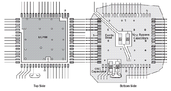
Microcomputer Grounds in One- and Two-Layer PCB Design
A microcomputer ground is a ground area on the bottom
layer underneath the microcomputer that becomes a ground
island for the noise made by the microcomputer.
This area should extend about 1/4 inch outside the outline
of the device and tie to the microprocessor ground. Ground
connections for the power-supply bypassing capacitors and
any bypassing capacitors on the pins also should tie to this
ground. Additionally, the ground area should extend out and
around the through holes for the oscillator leads, and the
bypass capacitors tied in to provide the smallest possible loop
area when viewed from the top.
The topside traces are shown in dotted line form on the bottom
side diagram for alignment purposes. Notice how the oscillator
capacitors lay back over the traces between the device and the
crystal. This eliminates loop area. The same is true for the
placement of the ferrite bead and Vcc bypass capacitor, being
centrally located with the main power lead running almost directly
under the lead finger for the ground.
PCB Design Guidelines For Reduced EMI
Texas Instruments
posted by kop @ 1:01 AM
![]()


<< Home