Electronic Device And Electronic Circuit

Data of electronic device , PCB Design and electronic circuit

Google
 
Web basicelectronic.blogspot.com

Monday, July 31, 2006

switching regulators for replace 78xx

The R-78xx-Series high efficiency switching regulators are ideally
suited to replace 78xx linear regulators and are pin compatible.


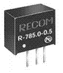
The efficiency of up to 97% means that very little energy is wasted as
heat so there is no need for any heat sinks with their additional space
and mounting costs. Low ripple and noise figures and a short circuit
input current of typically only 7mA round off the specifications of this
versatile converter series.


Features
- Efficiency up to 97%,Non isolated,no need for heatsinks
- Pin-out compatible with LM78XX Linears
- Very low profile( L*W*H=11.5*7.5*10.2 )
- Wide input range.(4.75V ~ 34V)
- Short circuit protection, Thermal shutdown
- Non standard outputs available as specials between 1.5V ~15.5V

- Low ripple and noise

www.recom-international.com

Sunday, July 30, 2006

Easy 32-Segment Driver circuit

This device is easy way for control 32-Segment display
by three control lines

AY0438 32-Segment CMOS LCD Driver
DESCRIPTION
The AY0438 is a CMOS integrated device that drives a liquid crystal
display, usually under microprocessor control. The part acts as a
smart peripheral that drives up to 32 LCD segments. It needs only
three control lines due to its serial input construction. It latches the
data to be displayed and relieves the microcontroller from the task of

generating the required waveforms.

Saturday, July 29, 2006

Remote I/O expander circuit

Each of the PCF8574’s eight I/Os can be independently
used as an input or output.

PCF8574
Remote 8-bit I/O expander for I2C-bus
The PCF8574 is a silicon CMOS circuit. It provides general
purpose remote I/O expansion for most microcontroller
families via the two-line bidirectional bus (I2C).

The device consists of an 8-bit quasi-bidirectional port and
an I2C-bus interface. The PCF8574 has a low current
consumption and includes latched outputs with high
current drive capability for directly driving LEDs. It also
possesses an interrupt line (INT) which can be connected
to the interrupt logic of the microcontroller. By sending an
interrupt signal on this line, the remote I/O can inform the
microcontroller if there is incoming data on its ports without
having to communicate via the I2C-bus. This means that
the PCF8574 can remain a simple slave device.

Address of PCF8574 can set at pin A0,A1,A2

slave addresses.

Thursday, July 27, 2006

Simple Input Port Expender Circuit

We can use PISO IC for increase input port of microcontroller
They can expender output port from three port to eight port


74LS165 are 8-Bit Parallel In/Serial Output Shift Registers
which shifts data in the direction of QA toward QH when clocked.
Parallel-in access is made available by eight individual direct data
inputs, which are enabled by a low level at the shift/load
input. These registers also feature gated clock inputs and
complementary outputs from the eighth bit.

C code for 74165

Tuesday, July 25, 2006

Simple Output Port Expender Circuit

We can use SIPO IC for increase output port of microcontroller
They can expender output port from three port to eight port

CD74HC4094 are 8-stage serial shift registers having a storage
latch associated with each stage for strobing data from the serial
input to parallel buffered three-state outputs.

Data is shifted on positive clock transitions. The data in each
shift register stage is transferred to the storage register when
the Strobe input is high. Data in the storage register appears
at the outputs whenever the Output-Enable signal is high.

Sunday, July 23, 2006

Resettable fuses

Polyswitch
A PolySwitch (also Polyfuse and Multiswitch) is a polymer form of

positive temperature coefficient resistor (PPTC) which acts as a self
repairing fuse.

"PolySwitch" is a registered trademark of Raychem Corporation. While the
generic term for these devices is sometimes called resettable fuses technically
these are not fuses but actually non-linear thermistors.

A PPTC has a current rating. When the current flowing through the PolySwitch
device, (which acts as a resistor) exceeds the current limit of, (for example)
100 mA, the PPTC device warms up above a threshold temperature and the
electrical resistance of the PPTC device suddenly increases from a few ohms
to a few kiloohms.

http://en.wikipedia.org/wiki/Polyswitch

Saturday, July 22, 2006

Simple delay time circuit

We can use series RC circuit and voltage comparator to generate
a time delay. Two resistors R2 and R3 are used as a voltage divider
which applies about two-thirds of the Vcc voltage to the positive
comparator input The delay time after the Vin change form low to
high will be around one time constant


Time constant = R1C1 = 100K * 10uF = 1 seconds.

The delay time can be adjust by adjusting R1 or change C1
..........................................................................................

Pogrammable digital timer circuit

Isolated Thermocouple Transducer Circuit

Labels:

Friday, July 21, 2006

Animated illustrations electronic circuit

If you interested in electronic circuit visit the website of
Paul Falstad.
This website includes java applet is an electronic circuit simulator.
Show animated illustrations of how electronic circuits work


http://www.falstad.com/circuit

Thursday, July 20, 2006

LM231

The LM231/LM331 family of voltage-to-frequency converters
are ideally suited for use in simple low-cost circuits for
analog-to-digital conversion, precision frequency-to-voltage
conversion
, long-term integration, linear frequency modulation
or demodulation, and many other functions


Features
- Guaranteed linearity 0.01% max
- Improved performance in existing voltage-to-frequency
conversion applications
- Split or single supply operation
- Operates on single 5V supply
- Pulse output compatible with all logic forms
- Excellent temperature stability, ±50 ppm/°C max
- Low power dissipation, 15 mW typical at 5V
- Wide dynamic range, 100 dB min at 10 kHz full scale
- Wide range of full scale frequency, 1 Hz to 100 kHz
- Low cost

Wednesday, July 19, 2006

Simple Frequency to Voltage circuit

Frequency-to-Voltage converter circuit can use LM331
(Precision Voltage-to-Frequency Converters) by circuit below
But out put form pin 1 of lm331 is current so we must be careful
Input impredance of circuit that connected with this circuit


Fin 10kHz full scale
Vout = Fin * 2.09V*(RL/Rs)*(Rt*Ct)

Monday, July 17, 2006

PWM generator circuit

A simple PWM (Pulse width modulation) generator circuit is
LM555 In ASTABLE OPERATION

ASTABLE OPERATION
Form circuit it will trigger itself and free run as a multivibrator.
The external capacitor charges through RA + RB and discharges
through RB. Thus the duty cycle may be precisely
set by the ratio of these two resistors.

In this mode of operation, the capacitor charges and discharges
between 1/3 VCC and 2/3 VCC. As in the triggered
mode, the charge and discharge times, and therefore the frequencyare

independent of the supply voltage.


- Top Trace: Output 5V/Div

- Bottom Trace: Capacitor Voltage 1V/Div.

The charge time (output high) is given by:
t1 = 0.693 (RA + RB) C
And the discharge time (output low) by:
t2 = 0.693 (RB) C
Thus the total period is:
T = t1 + t2 = 0.693 (RA +2RB) C
The frequency of oscillation is:
F = 1/T
The duty cycle is:
D = Rb/(Ra+2Rb)

4a-dc motor drive circuit

Labels:

Sunday, July 16, 2006

A one-shot timer circuit

A one-shot timer circuit or interval timer when input trigger pulse
applied. Out put will change to high and remain high until end of
delay time out put will change to low

This circuit used LM555 in monostable operation
The external capacitor is initially held discharged
by a transistor inside the timer. Upon application of a negative
trigger pulse of less than 1/3 VCC to pin 2, the flip-flop is
set which both releases the short circuit across the capacitor
and drives the output high.


During the timing cycle when the output is high, the further
application of a trigger pulse will not effect
the circuit so long
as the trigger input is returned high at least 10μs before the
end of the timing interval. However the circuit can be reset
during this time by the application of a negative pulse to the
reset terminal (pin 4). The output will then remain in the low
state until a trigger pulse is again applied.

Figure below is a nomograph for easy determination of R, C
Values for various time delays of lm555 timer

Saturday, July 15, 2006

Bidirectional Logic Level Translator

The ADG3304 is a bidirectional logic level translator that
con-tains four bidirectional channels.

It can be used in multivoltage digital system applications such
as data transfer between a low voltage DSP/controller and a
higher voltage device using SPI and MICROWIRE interfaces.

The voltage applied to VCCA sets the logic levels on the A side
of the device, while VCCY sets the levels on the Y side. For proper
operation, VCCA must always be less than VCCY. The
VCCA-com-patible logic signals applied to the A side of the device
appear as VCCY-compatible levels on the Y side. Similarly,
VCCY-compatible logic levels applied to the Y side of the device
appear as VCCA-compatible logic levels on the A side.

The enable pin (EN) provides three-state operation on both the
A-side and the Y-side pins. When the EN pin is pulled low, the
terminals on both sides of the device are in the high impedance
state. The EN pin is referred to the VCCA supply voltage and

driven high for normal operation.

ADG3304 FEATURES
Bidirectional level translation
Operates from 1.15 V to 5.5 V
Low quiescent current <>

Friday, July 14, 2006

CMOS to high voltage level translator

The ADG3123 is an 8-channel, noninverting CMOS to high voltage
level translator


DESCRIPTION
The internal architecture of the device ensures compatibility with logic
circuits running from supply voltages within the 2.3 V to 5.5 V range.
The voltages applied to Pin VDDA, Pin VDDB, and Pin VSS set the
logic levels available at the outputs on the Y side of the device. Pin
VDDA and Pin VDDB set the high output level for Pin Y1 to Pin Y6
and for Pin Y7 to Pin Y8
, respectively. The VSS pin sets the low output
level for all channels.
The ADG3123 can provide output voltages levels
down to −10 V for a low input level and up to +30 V for a high input
logic level. For proper operation, VDDB must always be greater than or
equal to VDDA and the voltage between the Pin VDDB and Pin VSS
should not exceed 35 V.

FEATURES
- 2.3 V to 5.5 V input voltage range
- Output voltage levels (VDDA and VDDB to VSS ≤ 35 V)
Low output voltage levels: down to −24.4 V
High output voltage levels: up to +35 V
- Rise/fall time: 12 ns/19.5 ns typical
- Propagation delay: 80 ns typical
- Operating frequency: 100 kHz typical
- Ultralow quiescent current: 65 μA typical
- 20-lead, Pb-free, TSSOP package

Wednesday, July 12, 2006

Analog Signal Multiplexing circuit

Analog Signal switching and Multiplexing circuit

CD4066B
CMOS QUAD BILATERAL SWITCH


CD4066B is a quad bilateral anaolog switch intended for the
transmission or multiplexing of analog or digital signals.
It is pin-for-pin compatible with the CD4016B, but exhibits
a much lower on-state resistance. In addition, the on-state
resistance is relatively constant over the full input-signal range.
The CD4066B consists of four bilateral switches, each with
independent controls.

- 15-V Digital or }7.5-V Peak-to-Peak Switching
- 125-Ω Typical On-State Resistance for 15-V Operation
- Switch On-State Resistance Matched to Within 5 Ω Over 15-V

Signal-Input

Tuesday, July 11, 2006

Analog signal isolation

This device can also be used for general analog signal isolation
applications requiring high accuracy, stability, and linearity
under similarly severe noise conditions.
Analog signal isolation circuit

HCPL-7840

Description
The HCPL-7840 isolation amplifier family was
designed for current sensing in electronic motor drives.
In a typical implementation, motor currents flow through
an external resistor and the resulting analog voltage drop
is sensed by the HCPL-7840.

Monday, July 10, 2006

LCDs connected to the uC

LCDs connected to the microcontroller in 4 bit data bus mode. LCD will require
a total of 7 data lines
3 control lines plus the 4 lines for the data bus in simple control LCD we will set

RW = 0(write only)

- The EN line is called "Enable."
This control line is used to tell the LCD that you are sending it data.

- The RS line is the "Register Select" line.
RS is low (0), the data is to be treated as a command or special instruction
RS is high (1), the data being sent is text data which sould be displayed on the

screen.

- The RW line is the "Read/Write" control line.
RW is low (0), the information on the data bus is being written to the LCD.
RW is high (1), the program is effectively querying (or reading) the LCD.


Saturday, July 08, 2006

External Watchdog Timer

The watchdog timer is monitors an I/O line from the
mC system. This line must be toggled once every interval time to
verify correct software execution. Failure to toggle the line indicates
that the mC system is not correctly executing its program
and may be tied up in an endless loop. If this happens, a reset
pulse is generated to initialize the processor.

ADM8690–ADM8695
The ADM8690–ADM8695 family of supervisory circuits offers
complete single chip solutions for power supply monitoring and
battery control functions in microprocessor systems. These
functions include mP reset, backup battery switchover, watchdog
timer, CMOS RAM write protection and power failure warning.
The complete family provides a variety of configurations to satisfy
most microprocessor system requirements.

Friday, July 07, 2006

Step-up Switching Regulation

The basic step–up switching regulator

Energy is stored in the inductor during the time that transistor
Q1 is in the “on”state. Upon turn–off, the energy is transferred
in series with Vin to the output filter capacitor and load.
This configuration allows the output voltage to be set to any
value greater than that of the input by the following relationship:
Vout = Vin( ton/toff) + Vin

step-up switching regulator by mc34063


mc34063

Thursday, July 06, 2006

Microcontroller programmer circuit

Connection pic microcontroller with PX-800 Programmer for download
hex code to pic microcontroller

microcontroller to RS-485circuit , digital potentiometers

Programmable Digital Timer circuit

Programmable Digital Timer circuit
A positive pulse on MASTER RESET resets the counters
and latch. The output goes high and remains high until the
number of pulses, selected by A and B, are counted. This
circuit is retriggerable and is as accurate as the input frequency.
If additional accuracy is desired, an external clock
can be used on pin 3. A setup time equal to the width of the
one-shot output is required immediately following initial
power up, during which time the output will be high.
f =1/(2.3 RtcCtc)
A = 0, B = 0 , COUNT = 8192
A = 0, B = 1 , COUNT = 1024
A = 1, B = 0 , COUNT = 256
A = 1, B = 1 , COUNT = 65535

t = COUNT / f

CD4541B
CMOS Programmable TimerHigh Voltage Types (20V Rating)
Description
CD4541B programmable timer consists of a 16-stage binary
counter, an oscillator that is controlled by external R-C components
(2 resistors and a capacitor), an automatic power-on
reset circuit, and output control logic. The counter increments
on positive-edge clock transitions and can also be reset via the

MASTER RESET input
Datasheet

Wednesday, July 05, 2006

Thermocouple Amplifier Circuit

Thermocouple amplifier circuit for convert signal form thermocouple to
voltage gain 10mV/?C


AD595
Monolithic Thermocouple Amplifier with Cold Junction Compensation
Pretrimmed for Type K Thermocouples


Product Description
The AD594/AD595 is a complete instrumentation amplifier and
thermocouple cold junction compensator on a monolithic chip.
It combines an ice point reference with a precalibrated amplifier to
produce a high level (10 mV/?C) output directly from a thermocouple
signal. Pin-strapping options allow it to be used as a linear
amplifier-compensator or as a switched output setpoint controller
using either fixedor remote setpoint control. It can be used to amplify
its compensation voltage directly, thereby converting it to a stand-alone
Celsius transducer with a low impedance voltage output
.

Datasheet

Tuesday, July 04, 2006

Circuit for receive signal 4-20mA

Differential amp are the simplest circuit for receive signal 4-20mA
where a signal source flow to resistor 100 ohm will create voltage has
both of its terminals biased at several volts above ground, you need to
amplify the difference between the terminals. What about noise that
adds an unwanted voltage equally to both terminals of a sensor?
The differential amp reject the noise and rescue the signal.

Filtering is done to eliminate unwanted content in signal
A low pass filter can be formed by placing a capacitor in the feedback
loop of a differential amp
gain stage

gain = R2/R1
fo = 1/(2*Pi*R2*C1)


Monday, July 03, 2006

Standard Resister Values

This is a typical standard value of resistor

1.0 - 10 - 100 - 1.0K - 10K - 100K - 1.0M - 10M
1.1 - 11 - 110 - 1.1K - 11K - 110K - 1.1M - 11M
1.2 - 12 - 120 - 1.2K - 12K - 120K - 1.2M - 12M
1.3 - 13 - 130 - 1.3K - 13K - 130K - 1.3M - 13M
1.5 - 15 - 150 - 1.5K - 15K - 150K - 1.5M - 15M
1.6 - 16 - 160 - 1.6K - 16K - 160K - 1.6M - 16M
1.8 - 18 - 180 - 1.8K - 18K - 180K - 1.8M - 18M
2.0 - 20 - 200 - 2.0K - 20K - 200K - 2.0M - 20M
2.2 - 22 - 220 - 2.2K - 22K - 220K - 2.2M - 22M
2.4 - 24 - 240 - 2.4K - 24K - 240K - 2.4M
2.7 - 27 - 270 - 2.7K - 27K - 270K - 2.7M
3.0 - 30 - 300 - 3.0K - 30K - 300K - 3.0M
3.3 - 33 - 330 - 3.3K - 33K - 330K - 3.3M
3.6 - 36 - 360 - 3.6K - 36K - 360K - 3.6M
3.9 - 39 - 390 - 3.9K - 39K - 390K - 3.9M
4.3 - 43 - 430 - 4.3K - 43K - 430K - 4.3M
4.7 - 47 - 470 - 4.7K - 47K - 470K - 4.7M
5.1 - 51 - 510 - 5.1K - 51K - 510K - 5.1M
5.6 - 56 - 560 - 5.6K - 56K - 560K - 5.6M
6.2 - 62 - 620 - 6.2K - 62K - 620K - 6.2M
6.8 - 68 - 680 - 6.8K - 68K - 680K - 6.8M
7.5 - 75 - 750 - 7.5K - 75K - 750K - 7.5M
8.2 - 82 - 820 - 8.2K - 82K - 820K - 8.2M
9.1 - 91 - 910 - 9.1K - 91K - 910K - 9.1M

.............................................................................
Microcontroller to RS-485 circuit
Digital Potentiometers

Sunday, July 02, 2006

4A DC Motor Drive Circuit

Driving DC motors with integrated circuits is simple.
It a good choose for small dc motor drive.
Resistor 0.1 ohm for current feed back
FR303 is fast recovery diode


L298
The L298 is an integrated monolithic circuit in a 15-
lead Multiwatt and PowerSO20 packages. It is a
high voltage, high current dual full-bridge driver designedto
accept standardTTL logic levels and drive
inductive loads such as relays, solenoids, DC and
steppingmotors. Two enable inputs are provided to
enableor disable thedevice independentlyofthe input
signals. The emitters of the lower transistors of
each bridge are connected together and the corresponding
external terminal can be used for the connection of
an external sensing resistor.Anadditional
supply input is provided so that the logic works at a
lower voltage.

Specification
- OPERATINGSUPPLY VOLTAGEUP TO 46 V
- TOTAL DC CURRENT UP TO 4 A
- LOW SATURATION VOLTAGE
- OVERTEMPERATURE PROTECTION
LOGICAL ”0” INPUT VOLTAGE UP TO 1.5 V
(HIGH NOISE IMMUNITY)

Datasheet